Last updated: August 23, 2026
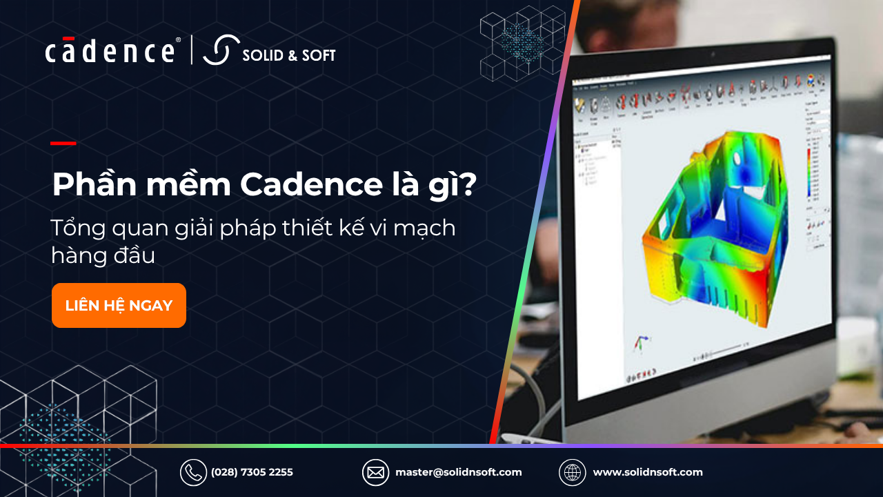
When exploring the semiconductor industry and hardware design, a common question asked by junior engineers is: what is Cadence software?
At its core, it is a comprehensive Electronic Design Automation (EDA) ecosystem developed by Cadence Design Systems.
This system provides specialized software and hardware solutions dedicated to integrated circuit (IC) design, printed circuit board (PCB) layout, and advanced chip packaging.
Understanding what Cadence software is helps electronics engineers bring complex circuit ideas to life, from initial RTL description down to generating GDSII files ready for manufacturing at semiconductor foundries.
Amidst the booming global semiconductor industry, mastering standard tools like Cadence is a critical success factor for any hardware design engineer.
The evolution of electronic design automation has completely transformed how modern microprocessors and system-on-chips (SoCs) are built. Without advanced EDA ecosystems, creating chips with tens of billions of transistors would be practically impossible. Engineers rely heavily on these tools to automate tedious layout tasks, run rigorous simulations, and verify that the silicon will perform correctly under extreme real-world conditions.
Furthermore, the integration of intelligent algorithms and machine learning features into modern EDA tools has significantly sped up design closure. Understanding what cadence software brings to the engineering table involves looking closely at both its historical foundation in custom analog layout and its current dominance in ultra-deep sub-micron digital implementation.
What is Cadence Software Used For: Core Product Lines Explained
The Cadence software ecosystem is divided into various specialized product lines, addressing each rigorous phase of the electronic product development workflow. Every tool in the Cadence software portfolio solves specific technical challenges in the semiconductor industry.
The Virtuoso product line within Cadence software is the gold standard for custom IC, analog, RF, and mixed-signal design.
Engineers use Virtuoso for schematic capture, simulation via Spectre Simulator, and transistor-level physical layout design.
The Genus and Innovus product lines play a primary role in digital IC implementation.
Genus performs RTL synthesis, translating VHDL/Verilog source code into logic gate netlists, while Innovus handles automatic Place and Route (P&R) with powerful optimization for leakage current and chip area.
The Allegro product line focuses on high-speed printed circuit board (PCB) design and advanced IC packaging.
Cadence Allegro software helps engineers manage complex constraint management, signal integrity analysis, and power integrity on high-layer boards.
To better understand the origins and global technology standards of these tools, you can explore direct information on the official website of Cadence Design Systems.
Beyond these primary suites, the ecosystem also encompasses advanced verification platforms such as JasperGold for formal verification and Palladium for hardware emulation. These verification solutions allow design teams to test software workloads on pre-silicon virtual prototypes, ensuring that software stacks are fully operational long before the physical silicon arrives back from the foundry. This seamless co-development of hardware and software is one of the primary reasons why leading technology companies standardize their entire engineering pipelines around this platform.
Why is Cadence Software the Top Choice for IC Design Engineers?
Cadence software maintains a massive market share in the global semiconductor industry due to its ability to solve increasingly severe physical challenges of advanced technology nodes.
As transistor sizes shrink down to sub-5nm and 3nm processes, physical phenomena such as crosstalk, IR drop, and thermal effects become critically severe.
Cadence software integrates advanced multiphysics analysis tools, allowing engineers to accurately predict the thermal and mechanical performance of integrated circuits from early design stages.
Tightly synchronized data sharing among tools within the Cadence software suite minimizes errors during handoffs between analog, digital, and packaging design teams.
Furthermore, Cadence software strongly supports international IP (Intellectual Property) standards and integrates deeply with major wafer foundries like TSMC, Samsung, and Intel Foundry.
This ensures that designs created using Cadence software maintain high reliability and achieve first-time silicon success.
Besides semiconductor design tools, hardware engineers frequently deal with PCB layout challenges. You can learn more about professional PCB design standards through our guide on the PCB design process on our website.
Another key driver for its widespread adoption is the robust support for signoff analysis. In advanced nodes, timing, power, and physical verification signoff must be absolute to avoid catastrophic multi-million-dollar re-spins. Tools like Tempus for static timing analysis and Quantus for parasitic extraction work in concert to ensure that every nanosecond and milliwatt is accounted for. Engineers trust these suites because their correlation with actual silicon measurements has been proven over decades across thousands of successful tape-outs.
Practical Applications of Cadence Software Across Tech Industries
Cadence software is widely applied in developing high-performance computing (HPC) chips, AI accelerators, mobile processors, and automotive ICs.
Major technology corporations and semiconductor startups alike rely on this system to significantly shorten their time-to-market.
In automotive IC design, Cadence software provides tool packages compliant with ISO 26262 functional safety standards, helping engineers verify hardware system reliability under harsh operating conditions.
In 5G communications and data center sectors, solutions from the company help optimize high-speed signal transmission lines exceeding tens of gigabits per second.
In practice, mastering the operation of these hardware design tools opens up tremendous career opportunities for young engineers.
Global enterprises constantly hunt for talent with a solid foundation in electronic design automation workflows.
Cadence not only provides software tools but also acts as a strategic technology partner, shaping standards for the global and fast-growing IC design industry.
As artificial intelligence and machine learning workloads surge, specialized AI chips require unprecedented levels of memory bandwidth and computational density. The platform’s advanced packaging solutions, such as 3D-IC design tools, enable heterogeneous integration where logic dies, memory stacks, and I/O interfaces are stacked vertically or placed side-by-side on silicon interposers. This capability keeps data moving quickly and efficiently, directly addressing the scaling bottlenecks of traditional 2D planar system architectures.
Conclusion: The Future of Semiconductor Engineering with Cadence Software
Looking ahead, the role of electronic design automation will only grow more vital as devices become smarter, faster, and more energy-efficient. Whether you are designing a low-power IoT sensor node or a massive cloud data center accelerator, knowing what cadence software offers and how to harness its capabilities is an indispensable skill for modern hardware architects.
By continually adapting to new manufacturing nodes, integrating generative AI into layout workflows, and fostering strong collaborative ecosystems with foundries and IP vendors, the platform remains at the very forefront of digital and analog innovation.
References
- Cadence digital design and signoff
- Cadence PCB design and analysis
- Cadence products
- Cadence multiphysics system analysis